Silicon Photonics Design
Pattern Generator for Silicon Photonics Design
"LightParts"
Simple operation to generate patterns for designing the silicon photonic devices. Generated patterns can be loaded directly to CAD software.
LSI Failure Analysis
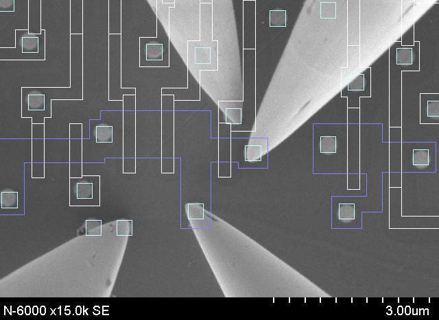
CAD Navigation System for Failure Analysis
"NASFA", "AZSA"
Improve TAT by using CAD data effectively to spot out location on the electron microscope image.
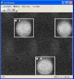
Cell Counting System
"Marrive"
Accurately count the repeated patterns of VIA (DRAM, SRAM, Flash, etc.) to increase your work efficiency.
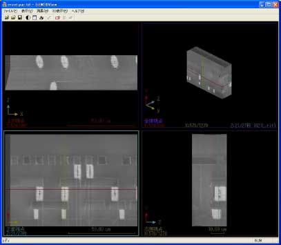
SEM 3D Viewer
"SEM3D"
Strongly support failure analysis by generating 3D image of LSI, and displaying
the cross-sectional image.
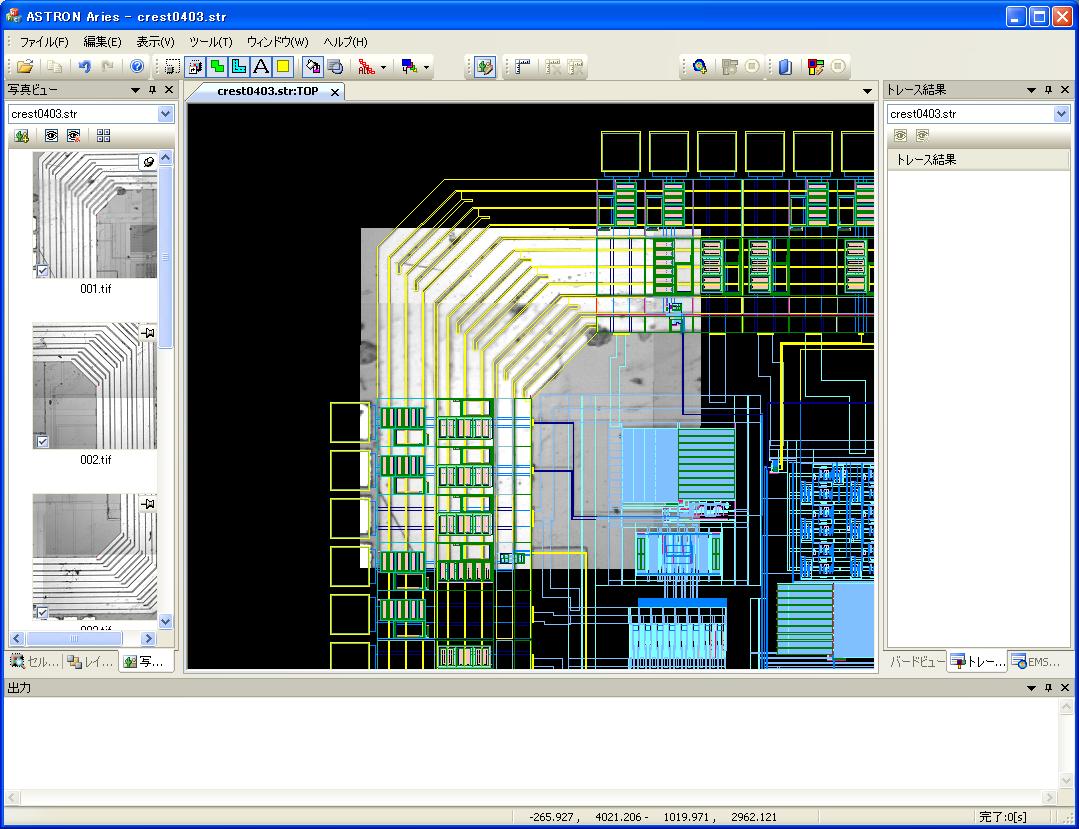
Offline CAD Navigation System
"Aries"
Enables to work on failure analysis of LSI at your own desk. Strongly support your work with useful functions, such as auto-layout of microscope images on CAD data.
LSI Design

High-Speed Layout Viewer
"SView/SView-PC"
High-speed loading and displaying of large layout data. Specialized for checking layout data, comes in handy in a variety of processes from LSI design, manufacture, and failure analysis.
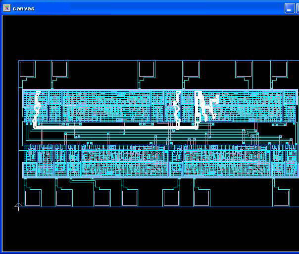
Netlist Extraction and Cross-Probing
"Neals"
Extract netlist from the layout, and cross-probe the circuit logic with the layout.
Data Conversion
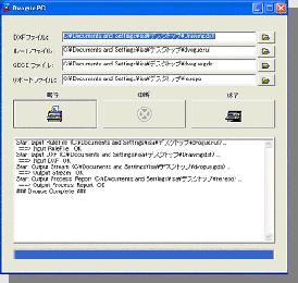
DXF to GDS Converter
"Dvogue"
Convert DXF format data to GDS format data, and generate masks from converted data.